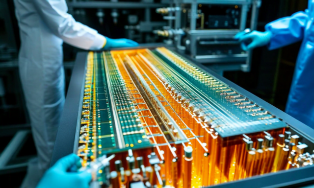
Every few months, a new GPU benchmark lands and the AI hardware conversation resets around flops per dollar. Transformer throughput. Attention head parallelism. These numbers matter. But the engineers actually building hyperscale AI clusters have a different problem on their minds: how do you move 400 terabits per second between racks without the datacenter turning into a heat engine?
Copper interconnects are the answer that works until it doesn't. At 400Gbps per lane — the current generation — signal integrity degrades over distances of more than a few meters. Power consumption climbs with the square of frequency. And the cables get physically unwieldy. When you're laying out a datacenter with 50,000 GPUs and trying to minimize all-reduce latency across the training cluster, the interconnect topology isn't a secondary consideration. It's the whole game.
What Silicon Photonics Actually Does
The pitch for photonic interconnects has been around for decades. Light doesn't have the same frequency-dependent loss as copper. You can multiplex multiple wavelengths on a single fiber and get bandwidth density that electrical cables can't approach. The physics is well understood. The problem was always manufacturing: getting optical components to integrate with CMOS processes at volume and cost.
That problem is substantively solved — not completely, not cheaply, but solved enough to ship products. Intel, Broadcom, and a wave of startups have demonstrated silicon photonics transceivers that co-package with switching ASICs and reduce interconnect power by 5x compared to equivalent copper solutions at 800Gbps. The key innovation is photonic integration — moving the optical engine close enough to the ASIC die that you eliminate the electrical-to-optical conversion losses that plagued earlier external transceiver designs.
Co-packaged optics (CPO) is the term of art. Instead of a pluggable transceiver on the front panel, you mount the photonic chip directly on the switching package. The electrical traces from ASIC to photonic die are millimeters long rather than centimeters. That shortens the path enough to make the power arithmetic work. Arista and Cisco both demonstrated CPO switch platforms in 2025. Volume shipments are happening now.
The Numbers That Make This Real
A conventional 51.2 Tbps switch ASIC with pluggable optics draws roughly 300-350W just for the optical components. A CPO design targeting the same throughput draws under 100W for optics. That's not a marginal efficiency gain — it's a datacenter-level shift in power density planning.
Hyperscale operators spend $3-5 billion annually on optics. Even a 30% reduction in optical power intensity at scale is a number that justifies complete infrastructure redesign. We've seen the detailed energy models. The projected savings are large enough that two major cloud operators have already announced CPO-first strategies for their next-generation AI fabric builds.
The second number worth understanding: a 1.6 Tbps CPO module occupying 8 optical lanes — what the industry calls 200G per lane — reduces thermal density at the port level by enough that you can double the switch radix before hitting cooling limits. More ports per switch means fewer switch hops in a fat-tree topology. Fewer hops means lower latency. For transformer models with all-reduce patterns that touch every GPU in the cluster, that latency reduction compounds across the entire training run.
Where the Investment Thesis Sits
We're not interested in the large established players executing this transition. Intel Photonics, II-VI, Coherent — they have the manufacturing scale but not the architecture velocity. The interesting companies are the ones doing photonic integration at the package level, building co-design tools that let ASIC architects and photonic engineers co-optimize the interface, and developing the testing infrastructure that volume production of photonic chiplets requires.
Photonic die test is genuinely hard. Electrical wafer probing is automated and mature. Photonic testing requires aligning optical fibers to sub-micron waveguide apertures at production scale. The companies solving yield-optimized photonic test will have durable competitive advantage that's invisible to most investors — it's infrastructure, not product, and infrastructure moats compound quietly.
There's also a materials dimension that gets under-reported. Silicon waveguides have nonlinearity and loss characteristics that limit certain applications. Lithium niobate on insulator (LNOI) modulators offer 10x lower drive voltage and dramatically higher bandwidth than silicon modulators. The fabrication challenges are significant, but several teams — including companies we're in discussion with — have working wafer-scale processes. LNOI won't replace silicon photonics broadly, but it opens applications in microwave photonics and co-integration with quantum systems where silicon's properties are limiting.
The Datacenter Isn't the Only Market
We focus primarily on datacenter applications because the TAM is large and the near-term procurement cycles are real. But the same photonic integration technology has a second life in LiDAR for autonomous systems, in coherent sensing for defense applications, and in the optical interconnect layers that future quantum-classical hybrid computers will require. That last one is a longer timeline, but it's not science fiction. The quantum error correction architectures that look most promising — particularly surface codes — generate enormous classical communication overhead. You need high-bandwidth, low-latency links between the quantum processor and the classical control hardware. Photonics is the only viable medium for that interface at scale.
We've been investing in this thesis for three years. What's changed is that the manufacturing maturity has crossed a threshold. The first silicon photonics products shipped in 2015. The CPO products shipping now are qualitatively different — higher integration, better yields, real cost competitiveness against copper at the relevant data rates. The market is moving from early adopter to mainstream procurement. That transition is when the interesting companies get built.
If you're building in photonics, silicon integration, or optical networking infrastructure, we'd like to hear from you. Reach the Coexin team.