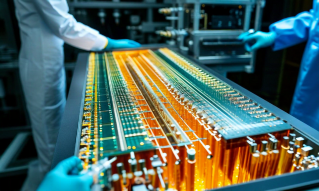
The transistor roadmap is in a genuinely uncomfortable place. The FinFET architecture — which enabled the scaling from 28nm down through 7nm — hits a fundamental wall below 3nm. Fin width needs to be smaller than the electron wavelength to maintain electrostatic control, and silicon simply doesn't cooperate at those dimensions. Gate-all-around (GAA) nanosheet transistors, which Intel calls RibbonFET and TSMC calls NSFET, extend the roadmap by stacking the channel nanosheets and wrapping the gate around all sides. It works. But it's also massively more complex to fabricate, and the electrostatic advantages shrink as the nanosheet stacks get thinner.
The alternative argument — the one that's been building in academic literature since the isolation of graphene in 2004, and particularly since MoS2 transistors were demonstrated in 2011 — is that the solution to short-channel effects in sub-5nm devices isn't 3D structure, it's a thinner channel. Specifically: a channel material that is atomically thin by definition, where thickness doesn't need to be controlled by deposition but is intrinsic to the crystal structure.
Why Thickness Matters
Short-channel effects are the core problem at advanced nodes. As the gate length shrinks, the electric field from the drain starts to influence the channel region that the gate is supposed to control. This reduces the transistor's ability to switch off cleanly, increasing off-state leakage current and power consumption. The fix is electrostatic: make the channel thinner so the gate's field dominates over the drain's.
Silicon channel thickness has to be controlled very precisely for sub-5nm operation — typically below 5nm, which means controlling material thickness at the 10-20 atomic layer level during deposition. That's extremely challenging for industrial-scale processes. Thickness variation causes threshold voltage variation, which causes yield loss.
Transition metal dichalcogenides (TMDs) — materials like MoS2, WSe2, and MoSe2 — don't have that problem. Their crystal structure consists of covalently bonded monolayers that naturally separate from each other via van der Waals forces. A monolayer of MoS2 is 0.65 nanometers thick. That's the channel. Atomically uniform, by physics rather than process control.
The Performance Picture
Monolayer MoS2 transistors have demonstrated subthreshold swings close to the theoretical 60 mV/decade limit at channel lengths below 5nm — something silicon struggles to achieve at those dimensions. The bandgap of MoS2 (~1.8 eV for monolayers) is larger than silicon, which is beneficial for suppressing off-state leakage. And the atomic thinness means the channel is almost entirely gate-controlled at short lengths.
The carrier mobility is lower than silicon, which means TMD-based transistors aren't going to win on raw switching speed at this point. But for applications where leakage power dominates — ultra-low-power IoT chips, implantable medical electronics, always-on sensor nodes — the tradeoff may favor TMDs significantly. At sub-10nm gate lengths, the theoretical picture for TMD devices actually shows competitive or superior performance to silicon in the relevant parameter space.
What the theoretical picture doesn't capture is manufacturability. Growing high-quality, large-area TMD films uniformly on standard silicon substrates is a materials science problem that hasn't been fully solved. Chemical vapor deposition (CVD) can grow monolayer MoS2 but grain boundaries in polycrystalline films degrade electrical performance substantially. Epitaxial growth of single-crystal films is possible but the substrate requirements and growth temperatures are not compatible with back-end-of-line (BEOL) integration at current nodes.
Heterostructures and Vertical Integration
The more immediately commercial argument for 2D materials isn't as the primary channel material replacing silicon — it's as a component in heterostructure stacks where the unique properties of multiple van der Waals materials are combined. Layer graphene (semimetal, excellent contact), a TMD channel, and a hexagonal boron nitride (hBN) gate dielectric, and you get a fully 2D transistor stack where every interface is atomically clean and the dielectric is a single-crystal insulator.
hBN is particularly interesting as a gate dielectric. Its large bandgap (~6 eV) makes it an excellent insulator, its atomic smoothness eliminates interface traps that plague amorphous oxides like SiO2 and HfO2, and its compatibility with TMD materials means you can build heterojunction devices with precisely controlled energy band alignments. Several groups have demonstrated near-ideal interface quality in graphene/hBN systems that exceeds anything achievable with silicon/oxide interfaces.
Tesseract Matter, our Cambridge-based portfolio company, is specifically working on scalable deposition processes for these heterostructure stacks — addressing the manufacturability gap rather than trying to push lab-scale demonstrations into fab production before the process is ready. That's the right approach. The material physics is not the open question. The process integration is.
What the Roadmap Looks Like From Here
IBM's roadmap shows 2D material integration as a potential option for sub-2nm nodes, contingent on solving the contact resistance problem (which is non-trivial — metal contacts to TMD channels have higher resistance than to silicon). TSMC's research publications mention 2D materials as a 1nm+ consideration. Intel's academic collaborations in this space have been quiet but consistent.
We don't think 2D materials replace silicon in leading-edge logic within this decade. The manufacturing readiness isn't there, and the installed base of silicon process expertise is enormous. The more likely scenario is that 2D materials appear first in specialized nodes — perhaps a dedicated back-end transistor layer for near-memory logic, or a specialized sub-threshold compute tier for ultra-low-power applications — before they challenge silicon in high-performance logic.
That still represents a significant investment opportunity. The companies building the CVD equipment, the process integration know-how, and the device characterization tools for large-area TMD films will matter enormously as this transition progresses. The fabs won't develop this internally from scratch. They'll acquire or partner with companies that have already solved the hard process problems.
If you're working on 2D materials, advanced dielectrics, or novel channel materials for next-generation transistors, we want to understand your work. Contact Coexin.