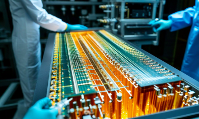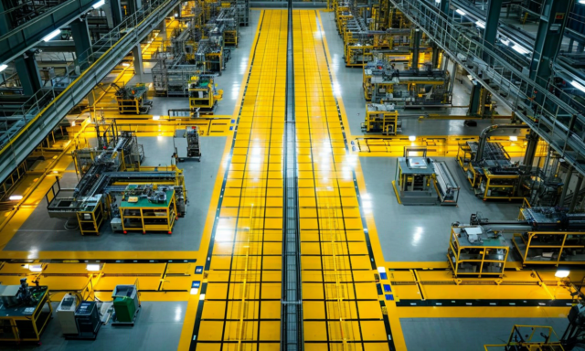
A leading-edge semiconductor fab runs 24 hours a day, seven days a week, processing wafers through several hundred distinct process steps. At each step — lithography, etch, deposition, CMP, implantation — something can go wrong. The critical question isn't whether there will be process excursions; there will always be excursions. The question is how quickly you detect them, how accurately you diagnose the root cause, and how surgically you correct without introducing additional variance.
Right now, that loop relies substantially on human engineers. Process control technicians monitor in-line metrology data, flag anomalies, and escalate to process engineers who decide whether to adjust recipe parameters, hold wafer lots, or reroute them. At 3nm and below, the acceptable process window — the range of parameters within which you get acceptable yield — is measured in fractions of a percent. The tolerance for human response latency shrinks accordingly.
This isn't a criticism of fab engineers. The best process engineers in the world work at TSMC, Samsung, and Intel Foundry. But the human nervous system wasn't designed to monitor 500 parallel process streams simultaneously and make optimal decisions under time pressure. Autonomous process control closes the gap between sensor data and corrective action in ways that are physically impossible with human-in-the-loop architectures.
What Autonomous Process Control Actually Means
Advanced process control (APC) has been a standard component of fab automation for decades. Run-to-run control adjusts recipe parameters between wafer runs based on metrology feedback. Fault detection and classification (FDC) algorithms flag equipment anomalies before they cause significant yield excursions. These systems are mature and widely deployed.
What's new is the combination of machine learning models trained on production data with the density of sensor infrastructure that modern fabs now have. An EUV lithography scanner generates gigabytes of equipment trace data per wafer lot. Etch tools have in-situ optical emission spectroscopy, wafer temperature maps, and endpoint detection signals. Deposition tools measure film thickness, uniformity, and stress in real time. The data density has outgrown what rule-based control systems can process effectively.
The companies we're most interested in are those building the inference layer between raw equipment data and actionable control decisions — specifically, systems that can identify subtle process drift patterns across correlated equipment parameters before those patterns manifest as measurable yield loss. The best systems we've seen can predict yield excursions 8-12 wafer lots ahead of when they would become visible in standard metrology, giving engineers time to intervene before scrap wafers happen.
The Robotics Layer
Process control is one dimension; physical material handling is another. Modern fabs use automated material handling systems (AMHS) to transport wafer lots between process tools in sealed front-opening unified pods (FOUPs). The AMHS architecture has been largely static for 20 years — a fixed rail system with programmatic routing. It works, but it's not adaptive.
The argument for autonomous robotics in fabs is that dynamic rerouting of wafer lots around bottlenecks and equipment downtime can improve fab throughput by 10-15% at current utilization levels. When an EUV scanner has an unplanned outage — which happens — a traditional AMHS queues wafer lots in front of the downed tool until engineering clears the fault. An autonomous system can dynamically reroute lots to alternative tools where the yield impact of slight parameter differences is within acceptable bounds, and flag which lots should wait versus which should move.
Seraph Robotics, our Pittsburgh portfolio company, is building precision robotic systems specifically for semiconductor fab environments — handling wafers at the 300mm standard with the positioning accuracy and contamination control that fab-grade handling requires. This is not general-purpose industrial robotics applied to a new setting. The environmental requirements (class-1 cleanroom compatibility, electrostatic discharge protection, vibration isolation) and the precision requirements (sub-micron placement repeatability) demand hardware designed specifically for the application.
The Yield Economics
The financial case for fab automation investment is straightforward. A leading-edge fab costs $15-20 billion to build and equip. At full utilization, it processes 50,000-100,000 wafer starts per month. A 1 percentage point improvement in yield on a mature 3nm process node is worth $200-400 million annually in additional revenue at current wafer pricing — that's per fab. The ROI math for automation investments that improve yield by even fractions of a percent closes quickly.
The more interesting number is the yield impact during ramp. New process nodes take 18-24 months to ramp from qualification yields (often 40-60%) to mature production yields (typically above 90%). Autonomous process control systems that accelerate the learning curve — that find and close process excursion modes faster — compress the ramp timeline. Compressing the ramp by 3-4 months on a $15 billion fab investment is worth hundreds of millions of dollars. The fabs know this, which is why process control automation is one of the fastest-growing categories of fab equipment spend.
Open Problems
The hardest remaining challenge in fab automation is explainability. When an autonomous system decides to adjust a key process parameter, the engineer needs to understand why. Black-box models that improve yield but can't explain their reasoning are a liability in a manufacturing environment where process qualification requires documented, traceable decisions. The companies building interpretable process control models — not just accurate ones — will have significantly better adoption in production fabs than those building opaque deep learning systems.
The second challenge is data quality and labeling. Training process control models requires labeled datasets that connect equipment sensor readings to wafer-level yield outcomes. Those labels come from inline and end-of-line metrology, and the correlation between a specific process step's equipment signature and the eventual yield outcome often requires integrating across dozens of subsequent process steps. Building the data pipeline infrastructure that correctly attributes yield outcomes to process root causes is as hard as building the model itself.
Working on process control, fab automation, or precision robotics for semiconductor manufacturing? We'd like to talk.